The best way to compare programming languages and what they offer is to program identical functionalities in the languages we know. I must admit that I am extremely concerned about the understanding of the following texts, but I cannot find a better and simpler way of complicated programming. An Arduino programmer does not understand what is behind Arduino functions. An AVR Studio C/C++ programmer does not understand what is behind assembler. An assembler programmer does not understand what is behind...
To understand all these programmers and therefore get to know the AVR architecture of microcontrollers, we must look at it from multiple programming languages. Because of the special characters of the C/C++ language ({ } [ ] < > * -> & | || && % ~ ^ << >> # ; : "" '), learning its syntax is repulsive and ugly. After a longer period of writing C/C++ syntax, brackets and special characters will not be a problem. On the contrary, it will be a phenomenal indicator of what starts, where it starts, where it ends, what it does, how it works... Assembler syntax is simpler than C/C++ syntax, and we will get to know it through examples.
In the previous text, the AVR registers were pictorially explained, their location in the address space of the SRAM memory, and their essential purpose. The first register we will get to know will be viewed at the assembler programmer level, and then delve into the understanding of the identical register from the perspective of AVR Studio C/C++ and the Arduino development environment. Therefore, let's forget about other programming languages for a moment and listen to what sounds like: DDRB.

If you try to pronounce the register name as a word, your tongue will likely get tangled somewhere between the letters. Try again, but this time like this: "Data Direction Register B." Not only can you say its full name, but you can also understand its purpose: "Register for controlling the data direction of Port B" (input/output). The DDRB register is 1 byte (8-bit) in size and can therefore only control 8 physical pins of the microcontroller (PB0 - PB7). Don't be surprised that almost everything in our microcontroller is 8 bits in size. The ATmega2560 is an 8-bit computer, so its registers are also 8 bits in size. The diagram shows the microcontroller pinout and the pins whose direction is controlled by the DDRB register.

As the ATmega2560 microcontroller has more than 8 pins, there are multiple DDRx registers. Their names differ only in the last letter, which describes the port: DDRA, DDRB, DDRC, DDRD, DDRE, DDRF, DDRG, DDRH, DDRJ, DDRK, and DDRL. After an AVR microcontroller reset, all of these registers are set to 0x00, and all pins of the microcontroller are inputs. This knowledge provides an important detail for controlling data direction: "If you want it to be an output, make it a logical 1." To configure input and output for the microcontroller, we always access the DDRx registers while following the mentioned rule (0x00 = inputs, 0xFF = outputs).
The biggest problem with Arduino functions such as pinMode() and all other Arduino functions is that you are limited to one architecture, the Arduino development board, and the Arduino IDE. If you know the DDRB register in the AVR architecture, you don't need to be afraid of the TIRISA register on the PIC or the FIO0DIR register on the ARM. The fact that registers have different names in different architectures and that they are controlled differently is not an insurmountable long-standing problem. A few days of searching through the documentation for another architecture will be enough to adopt new register names and their purposes.
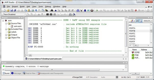
As the LED on the development board is connected to PB7, the following example shows how an assembler programmer can configure the output using the SBI instruction in a simple way.

The full name of the SBI instruction is "Set Bit", and it sets a desired register bit to logic "1". Only one instruction is required to set PB7 as the output of the microcontroller. However, the assembler programmer must be aware of an important limitation of the SBI instruction: the maximum address of the IO register that the instruction can handle is DEC 31 or HEX 0x1F.
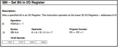
As the SBI instruction is 16 bits, only 5 bits can be used for the IO register address (0-31), and therefore it is not possible to use the instruction for an address greater than 0x1F. 3 bits, in combination with numbers (0-7), are used for the position in the register that we set to logic "1", and 8 bits are part of the operation code of the instruction (BIN 10011010). When we add all the bits together, we get a result of 16 (5+3+8). Remember: the AVR CPU only executes 16 or 32-bit instructions.
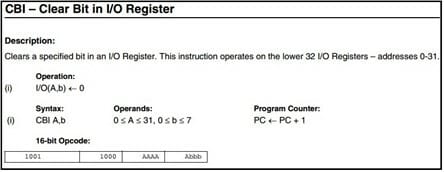
In addition to the SBI instruction, there is also the CBI instruction, which sets one bit of the IO register to logic "0". Note that the only difference between the CBI and SBI instructions is in the first 8 bits of the operation code. For CBI, they are 1001 1000, and for SBI, 1001 1010. The difference in just one bit of the operation code for the AVR CPU means the execution of a completely different instruction (SBI or CBI). The advantage of the CBI and SBI instructions is their speed in managing a single bit in the address space of IO registers 0-31. All other methods are slower because they require more instructions.
Executing CBI and SBI instructions requires 2 cycles of the main oscillator. If the MCU is running at 16 MHz, it can be said that configuring the output of port PB7 takes 2 x 62.5 ns or 125 ns (nanoseconds). It is important to know the duration of assembler instructions to have a better understanding of how much time is wasted when using "delay()". During the execution of one command of a higher programming language such as "DelayMs(1);", PB7 can be configured as the output of the microcontroller 8000 times.
SBI and CBI instructions can be used to control a single bit in a register, and in addition to being limited to only the first 32 IO registers, they are not suitable for controlling the entire register, i.e., 8 bits. If you wanted to set all 8 bits of the DDRB register as output, you would have to execute SBI 8 times. The following example shows how to set all bits of the DDRB register using the SBI instruction. (DDRB = 0xFF)
When accessing all bits of a single register, it is better to use the IN and OUT instructions. The example shows how to set all 8 bits of Port B as outputs (DDRB = 0xFF). When using the IN and OUT instructions, it is important to note that the maximum address of an IO register that can be read and written is 0x3F. Therefore, these instructions can only access IO registers in the address space of 0-63.

The IN and OUT instructions are a bit more complicated than CBI and SBI as they use the AVR's working registers, which we haven't discussed yet. The AVR architecture has 32 working registers, R0-R31, and we won't go into detail about them at the moment. Writing 0xFF to the DDRB register using the OUT instruction can be done by loading the constant into a working register, R16-R31, using the LDI instruction, and then using the OUT instruction to store the value of the working register at the address of the DDRB register. When writing to the DDRB register in this way, we follow this procedure:
Load the constant binary number 1111 1111 into a working register R16 (LDI R16, 0xFF).
Store the working register R16 at the address of the DDRB register (OUT DDRB, R16).
The OUT instruction has a significant drawback when it comes to manipulating a single bit: "With the OUT instruction, we change all 8 bits, not just one bit." If we want to change only one bit, we must know the state of the other 7 bits in order to keep them identical. The following example shows how to configure an output on port PB7 using the IN and OUT instructions, changing only one bit of PB7.

Controlling a single bit in C/C++ language is identical to controlling a single bit in assembly language using IN, OUT, ORI, and ANDI instructions. Since this chapter is more extensive, we will deal with the issue of the last example in the following text. ORI and ANDI instructions are logical operations OR and AND between a working register and a constant.
Let's remind ourselves: "AND and OR are logical operators whose truth tables we have memorized for the needs of digital electronics, but we have never found their purpose". We will dedicate the following text to "OR" and "AND" logical operators to understand controlling a single bit in both assembly and higher-level programming languages. We can describe the last example briefly in four steps:
Load the DDRB register into the working register R16.
Execute the OR operation of the R16 register with the constant HEX 0x80, BIN 1000000
The result of the operation is stored in the R16 register
Save the R16 working register at the address of the DDRB register
For better understanding of the assembly instructions SBI and CBI, it is good to try to control the PORTB register after configuring the DDRB register as an output. By changing the bits of the PORTB register, the microcontroller output is set to "0 V" or "5V", making it easy to understand the basic operation of the microcontroller output at the assembly level. To set the PB7 output and turn on the LED, only the "SBI DDRB, 7" and "SBI PORTB, 7" instructions need to be executed.

Top comments (0)