Last week I discussed BPU registers which store pointers and currently executed commands. Today's subject will be to introduce counting by designing an Arithmetic Logic Unit capable of addition and subtraction.
What's ALU again?
A short recap
An Arithmetic and Logic Unit is a part of the CPU that performs arithmetic and logic operations (naming remark: if it only does arithmetics the "and" in the name is dropped). Using control signals the CPU supplies ALU with data, selects the operation to be performed and takes the output. CPU does not directly control what logic happens inside.
The BPU executes Brainfuck Assembly Language commands, which only require two operations: addition and subtraction. My ALU will therefore be very simple; it will still require two data inputs and signals to control them, as well as the output signal and the operation select signal. All this I/O is present in any ALU, though.
Exterior design
Thinking outside the box
In designing complex logic systems it's important to start with their inputs, outputs and control signals.
It might be impossible to design them first, because it's necessary to start with considering internal design, as inputs, outputs and control signals may be determined by it.
Usually though circuits are designed as components of a bigger machine or as a side component communicating with the others so some inputs and outputs can be designed before even thinking about internal logic.
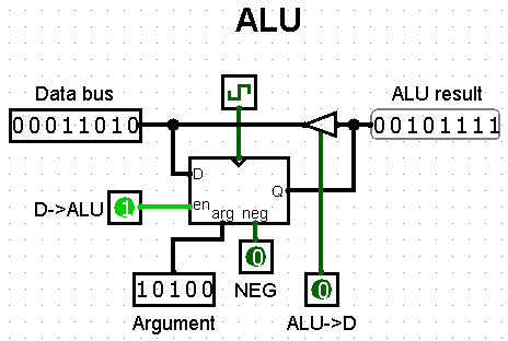
In this case the ALU is a part of the BPU and has a specified function. This is what the ALU's operation can tell about its inputs and outputs:
- The ALU must take a number from the data bus when needed and remember it.
- Data input from the data bus
-
D->ALUcontrol signal to control the input - A register inside to store data
- The ALU must add or subtract the argument from a specific remembered number.
- Data input from the command's argument
-
NEGsignal to select addition or subtraction - addition/subtraction circuit inside
- The ALU must output the outcome of this operation to the data bus when needed.
- Data output to the data bus
-
ALU->Dsignal to control the output
- All this functionality must be synchronised with the BPU.
- clock signal input
As you can see, knowing how the circuit is supposed to work and what it communicates with dictates all its inputs and outputs. This knowledge is enough to design the exterior of the ALU, but the bulk of work lays inside.
Binary addition and subtraction
How to reuse circuits
I will not describe interior design of a binary adder circuit, as it would be as long as this article itself. Long story short, it consists of cells that take two input bits (one from each number) and a carry bit from the previous cell and calculate the output and a carry bit for the next cell. It's like adding with carry on paper but using binary instead of decimal.
It is possible to design a similar cell system for subtraction and then decide which one to output based on the NEG signal, but if you tried designing such subtractor you would find that it only differs from the adder by one NOT gate: the first input is negated before calculating the carry. With this knowledge it is better to add some conditional processing to the adder instead of doubling its size with a separate subtractor.
Calculating a - b is just like a + b but with a flipped for carry calculation. This sounds like an easy fix, but without access to the interior of an adder I can only flip a for all operations - both carry and result calculations. Fortunately this is OK, as it results in a flipped subtraction output which can be flipped again to get the correct answer.
It turns out that all that is required for the addition/subtraction module is an adder and some conditional flipping which can be easily achieved with a XOR gate. If the first input to this gate is 0 then its output is equal to its second input, otherwise it outputs an inverse of the second input.

Internal ALU design
We're almost there
With all this information it's now finally time to design the full ALU circuit. Its inputs are: data from the data bus, data input enable signal, command argument to add/subtract, the NEG signal and the clock. ALU->D signal is used outside of the ALU, as shown on the diagram above. The circuit has one output, called Q, which is the result of the operation over the argument and the remembered value.
First, the ALU needs to remember input data from the data bus. This is achieved by passing it to a register enabled by the en signal and connected to the clock. Next, the contents of the register and the argument are passed through the adder/substractor and the result goes to the output Q. The finished circuit looks like this:
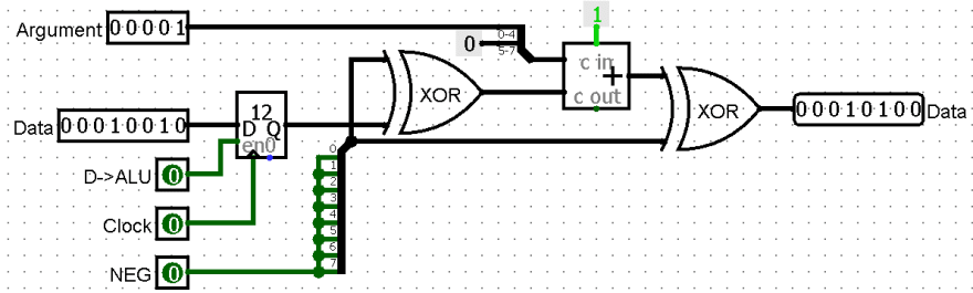
There are two more things I yet have to mention: The smaller one is that the argument must be expanded from 5 to 8 bits by prepending zeroes to be compatible with the 8-bit adder.
The bigger one is that the adder's carry input must be set to constant one. This follows from the fact that the argument is compiled as n-1 if the program is supposed to add/subtract in BAL. It is easy to compensate for that loss by tying carry bit high.
Conclusion
That's all, folks!
This week I've stepped through the process of designing a basic ALU. If you have any questions or requests feel free to ask in the comments. Tune in next week for the last big circuit and the brain of the BPU: a Command Decoder.

Top comments (0)