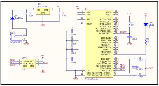
At the moment when I provide a stable power supply voltage, stable reset line, and stable operating frequency, the AVR microcontroller becomes a perfectly functional system. The only drawback of such hardware is the fact that the microcontroller does not do anything useful. To make the microcontroller useful, we must modify its memory. There are several ways to modify the memory of a microcontroller and several types of memory that we can modify. In-System Programming (ISP) is the most commonly used method for programming AVR microcontrollers and it consists of 6 programming lines (MOSI, MISO, SCK, RESET, GND, and VCC). Since I used the ATMEGA8A as an example of basic hardware needs, I will use it for the final hardware design as well as for the presentation of microcontroller memories. The lines of the ATMEGA8A microcontroller that need to be connected to the programmer are shown in the picture.

To be able to program the memories of AVR microcontrollers, it is necessary to provide voltage supply on the GND and VCC lines. There are USB programmers that have the option of supplying power to the microcontroller via USB voltage of 5V, but a better option is to supply the AVR from a voltage regulator. We can design AVR hardware to operate at 3.3V and use various components that operate at a maximum voltage of 3.6V. If we were to power such hardware from a USB programmer (5V), we would destroy all components that cannot operate at 5V. ISP allows us to program the AVR in-system, which means that we do not have to physically separate it from other electronics. It is enough to connect the ISP programmer to the finished device, turn on the device's power supply, and write the new memory state. The image shows two standard ISP connectors.
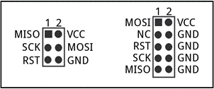
If we compare the pin names again, there are only 6 pins, so it is better to use a smaller connector (2x3) to save space. There are programmers that have a 2x5 connector, so a converter is needed to connect them to the finished hardware. In some AVR microcontrollers, ISP is connected in a different way. As an example, I mention the ATMEGA64 which uses PE0 and PE1 for the MOSI and MISO pins. This is stated in the technical documentation, but only on page 306 titled "SPI Serial Programming Pin Mapping". You will not often find an AVR microcontroller that uses different pins for ISP, but it is enough to remember that it can happen. If you want to be sure about the ISP pinout, read the technical documentation. We have only 3 pins where we can make a mistake. GND and VCC are power supply pins, RESET is unique. Three pins remain, MISO, MOSI, and SCK. In almost all AVR microcontrollers, we connect them to pins with identical names, MISO, MOSI, SCK. But beware, ATMEGA64 may not be the only black sheep.
When programming a microcontroller via ISP, there is another important rule: "The frequency of the ISP programmer must be lower than ¼ of the frequency of the AVR microcontroller." If we are programming ATMEGA8A for the first time, we need to know that it operates on an internal oscillator of 1 MHz and that the programmer's frequency must be lower than 250 kHz. This parameter can be set in the programmer's settings. When programming the microcontroller, it is necessary to set the MCU name, the file we want to program, and the memory we are programming. These settings are intuitive, so I won't describe them in detail right now. Many programmers will tell you that programming is problem-solving. Problems do not have to be mathematical in nature and directly related to program logic; they can also be related to the frequency of the ISP programmer. That's why I am listing these finer details that are a common problem but are relatively small in the documentation. To give our hardware some purpose, I added an LED to it, at least so we can turn it on or off. The final schematic and hardware design using the ATMEGA8A microcontroller are shown in the picture.

Using an ISP programmer, it is possible to modify the following memories:
• FLASH (8192 bytes)
• EEPROM (512 bytes)
• FUSES (2 bytes)
• LOCKBITS (1 byte)
It is not possible to permanently store data in SRAM memory and therefore we cannot program it. After turning off the device from the power supply, everything stored in SRAM memory will be forgotten.
The LOCKBITS memory of 1-byte size is used to lock the program and permissions around instructions (SPM, LPM) that can write and read FLASH memory. After writing FLASH, EEPROM, and FUSE memories, it is possible to lock the MCU to protect the written program from memory reading and device copying. A locked microcontroller is not permanently inaccessible, so using the programmer, an "Erase Device" can be performed which will set the FLASH, EEPROM, and LOCKBITS memories to 0xFF and allow us to program all memories again.
The FUSES memory, which is 2 bytes in size, is used for microcontroller operation settings such as clock selection, low-voltage protection, starting address of FLASH memory after reset, bootloader size, WDT protection, and more. This is the only memory in which we cannot make a mistake. In the FUSES memory, it is possible to disable the external RESET pin, and if you do so, the MCU will become inaccessible for ISP programming. We also set the clock of the microcontroller in the FUSE memory, so it is possible to accidentally select "External Clock" and make the MCU inaccessible again. It is also possible to set the clock to "External Crystal," but if you have not connected an external crystal oscillator in hardware, the MCU becomes inaccessible again. An HV parallel programmer can access the microcontroller regardless of any mistakes made, but it is cheaper to buy another microcontroller than a parallel programmer. In the example of the ATMEGA8A hardware, we can select "External Crystal" for the clock to make the MCU run at a maximum speed of 16MHz. The FUSES memory is not identical for all AVR microcontrollers, so it is best to rely on the technical documentation of the microcontroller for its configuration.
The EEPROM memory with a size of 512 bytes is most commonly used to store variable data that we want to preserve even when the device is turned off. If we want to make a device that counts every time it's turned on, obviously we need to store information about the number of device turn-ons somewhere. EEPROM memory is ideal for storing such information. We can use it to store the device name, various parameters on which the program is executed, the device password that the user can change, etc.
The FLASH memory with a size of 8192 bytes is the largest memory of the microcontroller. Everything we program, regardless of the programming language, ends up in the FLASH memory as a combination of "0" and "1". With all other memories, things are pretty simple. We store something in the EEPROM or SRAM memory and read back the identical data, but the data in FLASH memory is far more complex. The FLASH memory contains instructions for the CPU, and everything the microcontroller does comes down to executing the instructions in the FLASH memory. To better understand the role of FLASH memory, I will explain the execution of the simplest and largest program called "New Microcontroller". I won't call it empty because in digital electronics, we only know the states of memory "0" or "1". The new ATMEGA8A microcontroller is shipped with the FLASH memory state where all bits are set to logic "1". If the ATMEGA8A has 8192 bytes, it is easy to calculate how many different states of "0" or "1" can be stored in the FLASH memory.
8192 byte*8 bit=65536 bit
If you take a new Word document and use the copy/paste method to print 65536 logical "1"s, you will have the most precise insight into the FLASH memory of the purchased ATMEGA8A microcontroller. The AVR CPU only knows 2 types of instructions, those that occupy 2 bytes and those that occupy 4 bytes of FLASH memory, the third case does not exist. You can find all instructions for the AVR CPU and their encoding in the purest form of the combination of "0" and "1" in the document called "AVR Instruction Set". The laziest assembler instruction you can find in the aforementioned document is called "NOP" or "No Operation". We call it the laziest instruction because "NOP" does absolutely nothing, except that it takes one clock cycle of the microcontroller to execute the instruction. If the AVR executes one instruction for 62.5 ns at 16 MHz, "NOP" serves only to waste time. All high-level language instructions such as "Delay" and "Wait" are essentially identical to the assembler instruction "NOP". However, the microcontroller does not understand the instruction name "NOP" because the CPU executes only combinations of "0" and "1", and even such an instruction has an encoding that is understandable to the AVR processor. The "NOP" instruction in FLASH memory is recorded as 16 zeros, truly shown like this: "0000 0000 0000 0000". The instruction is 2 bytes long, which corresponds to the rule that the CPU only understands instructions that are 2 or 4 bytes long. The FLASH memory of the purchased ATMEGA8A consists of 65536 logical "1"s, not "0"s. What is the difference? Almost none, the instruction that is recorded as 16 zeros is called "NOP", and the instruction that is recorded as 16 ones is not an instruction at all. The microcontroller is absolutely indifferent as to whether it executes the instruction of 16 zeros or 16 ones, it will execute both combinations as the "NOP" instruction. The only difference is in our understanding and presentation of the instruction. 16 zeros are called "NOP", and 16 ones are called "Unknown Instruction". The image shows the FLASH memory of the purchased ATMEGA8A microcontroller:
If we consider FLASH memory in which all bits are set to logic "1", the microcontroller will execute the laziest instruction "NOP". This realization leads us to the conclusion that the microcontroller is still doing something, even when it is not doing anything useful. It will execute the first 2 bytes of logical "1s" and do "Nothing", then take the next 2 bytes of logical "1s" and again do "Nothing". We can analyze the instructions all the way to the end of FLASH memory and execute "Nothing". The microcontroller is still a limited computer that, when it reaches the end of FLASH memory, starts executing the same program again. You might be wondering, how long does it take for a new ATMEGA8A microcontroller to execute the entire FLASH "Nothing"? The purchased ATMEGA8A operates on an internal oscillator with a frequency of 1 MHz, and it takes 1 microsecond to execute one instruction. If we have 4096 instructions per 2 bytes, and each of them takes 1 microsecond, the AVR needs 4096 microseconds to execute all FLASH memory instructions. After the last instruction is executed, the program returns to the beginning of FLASH memory and the "Nothing" circus starts again. Even a microcontroller that you can call "empty" executes the most programs, and you will never use it to execute all FLASH memory instructions in such an extensive way. Okay, the program does nothing, but you must agree that such a program takes up the entire FLASH memory because it executes all possible "Nothing" instructions. All programs you write in life will never use the entire FLASH memory like our new microcontroller. Now, whether you consider the new microcontroller full or empty, is up to you. I would say it's full, full of nothing.
It is easy to analyze FLASH memory when it comes to the "NOP" instruction. The real complications come with writing a program that has a purpose, i.e., the program we program. All 130 assembly instructions are recorded as 16 or 32 bits in a combination of "0" and "1". It is terribly tedious to analyze such FLASH memory. To make matters worse, no written program executes instructions in the order of FLASH memory. We often check, compare, and condition something, so the results of operations scatter us throughout FLASH memory. The picture shows the beginning of FLASH memory of a program written in C and translated into assembler (HEX format).

A knowledgeable expert in AVR architecture will immediately know that the first instruction "10C0" skips the ISR vectors and redirects the program to the 15th or 20th instruction, depending on how many vectors the MCU has. We don't currently need to know what ISR vectors are or why the first instruction skips them. It is enough to conclude that the already complicated FLASH memory layout becomes even more complicated by the fact that instructions are not executed in order. There is nothing more complicated in microcontrollers than analyzing FLASH memory and the instructions that the MCU executes. It is much easier to write a completely new program than to understand what the microcontroller is doing at the FLASH memory level.
With this description of the basics of hardware and memory, I conclude the introductory text on microcontroller programming. In the next text, we can start with ARDUINO and programming in C/C++. Regardless of how much I write about programming in higher-level languages, I will often return to the smallest details of the AVR architecture, just so we can objectively look at all programming languages and better understand the true operation of the microcontroller.

Top comments (0)