Last week I showed you the parts of design of the brainfuck computer that work outside of the BPU: memory and simple input/output systems. Today I'll tackle the BPU itself by setting up some essential registers and signals to control them.
What are registers again?
A quick recap
A register is a circuit that can store an amount of bits, broadcast their contents and synchronously (on a rising or falling edge of the clock signal) overwrite it's contents with new data. Registers can be augmented with additional circuitry to create counters or shift registers.
In CPUs, registers contain various data about the state of the machine, for instance a currently executed command, addresses of relevant places in memory or intermediate values of arithmetic operations. You will find examples of all these use cases in the BPU, although today I will only tackle the first two: storing commands and addresses.
Program Register
What the BPU is currently doing
BPU commands will require multiple clock cycles to execute, mostly because only one memory address is accessible at a time and BPU accesses the memory a lot. This creates a need for the PR: a register that stores the currently executed instruction and loads the next one when it's finished.
As you may recall, compiled BAL words consist of a brainfuck command and it's argument. My BPU will use a variant of BAL that stores the command in the low bits of the word and the argument in the high ones. For 8-bit words it will look like AAAAACCC.
Since complementary commands have command numbers which differ by 1, their codes only differ by the lowest byte - 0 for commands that add (+>[) and 1 for commands that subtract (-<]). This allows me to create my first control signal, NEG, just by separating the lowest bit of each command, making the word structure AAAAACCN.

PR requires only one control signal called D->PR which enables synchronous loading data from the data bus. PR's output is split into three parts: the argument, the command and the NEG signal which is also part of the command. These signals will be interpreted by other components to make the BPU execute the correct command.
Data Pointer
What the BPU is looking at
Brainfuck operates on a linear memory using a pointer (called Data Pointer) that moves left and right. This DP is changed by commands > and <. Therefore it needs a two-way connection to the data bus to pass its contents to the ALU to add to or subtract from it and to load its contents after modification. It also needs to connect to the address bus to perform its task of pointing at a cell.

Because of all these bus connections the DP requires three control signals to operate:
-
D->DP- Just like in the PR it enables loading from the data bus -
DP->D- Broadcasts contents of the DP to the data bus -
DP->A- Broadcasts contents of the DP to the address bus
It is also connected to the Reset signal which, like the clock, is not generated by the BPU and comes from the outside. When this signal goes high the whole BPU is set to the starting state with all pointers set to zero and ready to load its first instruction. The PR didn't require this signal because the first thing the BPU should do after a reset is load a new command which overwrites contents of the PR anyway.
Program Counter
How the BPU knows what to do next
Another pointer the BPU will need is the PC which remembers position of the next command to execute. I will store it in a special variant of a register called a counter, which allows for easy incrementation of the value stored in it. This way I won't need to use the ALU to add 1 to the PC every time the BPU fethes a new instruction; however I will need to facilitate jumps, so connection to the ALU via the data bus is still required.
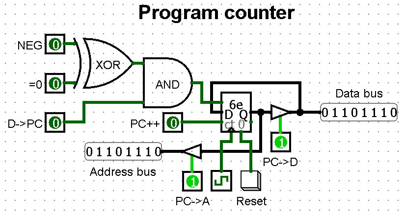
Standard PC operation requires three signals similar to DP signals:
-
PC->D- Broadcasts contents of the PC to the data bus -
PC->A- Broadcasts contents of the PC to the address bus -
PC++- Increments the PC on the rising edge of the clock
In addition to these PC has to load data from the data bus to do conditional jumps. Because jumps depend on a condition and the condition depends on the direction of the jump ([ jumps forward if the cell is 0, ] jumps backward if the cell is not zero) data loading is governed by three separate signals:
-
=0- Flag showing whether the currently selected cell is equal to zero -
NEG- The lowest bit of the command representing jump direction: 0 if command is[and 1 if command is] -
D->PC- Conditionally loads the contents of the data bus to the PC
All these signals need to be combined to create a single load signal for the counter. How? Firstly, the chip should load when the D->PC is on AND a certain condition is met, which already gives us the first logic gate to use. Then let's look at when said condition is met. If the command is [ then NEG is 0 and the condition is "jump when zero". On the other hand if the command is ] then NEG is 1 and the condition is "jump when not zero". This means that the condition is met when NEG and =0 are different, and this behaviour can be achieved with a XOR gate. The final operation is D->PC AND (NEG XOR =0) which you can see on the diagram.
Conclusion
I'm not finished yet
This week I've shown you the circuitry needed for necessary BPU registers and set up first internal control signals that will govern the BPU's operation. Next week I'll design a simple ALU to do something with contents of these registers.
Post Scriptum
News, credits & stuff
The big announcement is that I now have a proofreader! janekjan is my old friend and his English is way better than mine, so I'm very happy that he agreed to help me. Blame him for all the mistakes in the text now.
Another important news is that the BPU now has a github page! It is public and will contain all the materials for this tutorial, which currently means the Logisim file with all the designs. At some point in the tutorial I will make stuff like a compiler or some example programs and they will surely end up on this repo.
Final note: I see people reading my articles and some of them even leave hearts, but I could use some feedback. The question is how do you find the difficulty level of my tutorial? Should I perhaps explain in more detail how the components I'm using work? Maybe you would like to hear more about how I come up with the Logisim designs? Or possibly I spend too much time explaining the basics and you would rather just jump into the final designs? Share your thoughts in the comments.

Top comments (0)